PRESS RELEASE
Advanced Packaging in Europe's Semiconductor Ecosystem
The semiconductor industry is undergoing a pivotal transformation. Pack4EU and Blumorpho are driving innovation and sustainability to foster advanced packaging technologies
Driving Collaboration in Semiconductor Advanced Packaging
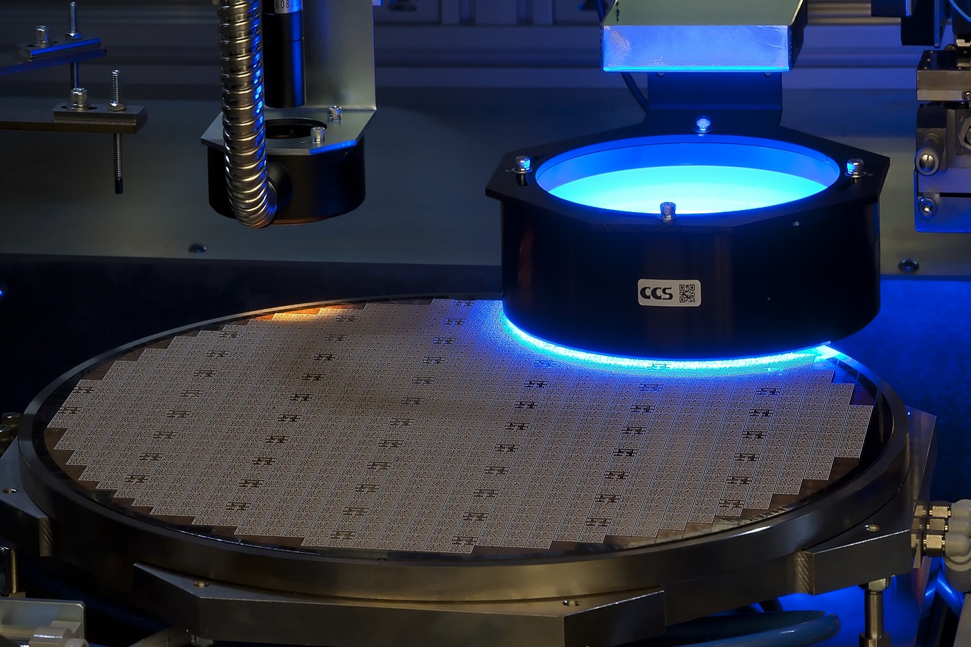
courtesy of Amkor
The semiconductor industry is undergoing a pivotal transformation, with advanced packaging technologies playing a critical role in enhancing performance and reducing development costs. In this context, Pack4EU, a consortium of key players in Europe’s semiconductor ecosystem, has emerged as a driving force, uniting stakeholders across the continent to focus on advanced packaging.
Key Technologies in Semiconductor Packaging: Chiplet Architecture, 2.5D/3D Integration
Chiplet Architecture
The traditional approach to semiconductor design typically involves integrating intellectual property (IP) blocks onto a single chip, referred to as a System on Chip (SoC). However, this approach is reaching its limits due to the increasing die size, which now exceed reticle sizes, and skyrocketing development costs. Chiplet architecture is redefining semiconductor design by allowing the integration of smaller, specialized chips into a single package. This is a change of paradigm from the System on Chip to a System on package. This modular approach addresses the limitations of Moore’s Law, enabling higher performance and flexibility in design.
However, challenges such as signal integrity, power efficiency, and thermal management remain
2.5D/3D Integration
2.5D and 3D advanced packaging allow multiple chips to be stacked within a single package, achieving greater density and performance. These technologies are essential for computing and AI but are also important for applications requiring highly integrated systems, such as ADAS, AI, and 6G telecommunications. In 2.5D packaging, interposers enable the interconnection of chiplets with high bandwidth and low latency, while 3D integration involves stacking dies to achieve even higher density.
The European Research Community is actively developing these technologies, focusing on challenges like thermal management, interconnect bandwidth, and signal integrity. A key component of this strategy is the development of Pilot Lines and a Design Platform. These initiatives are critical to building a strong European semiconductor value chain. The aim is to support Research in the development of heterogeneous integration technologies for diverse markets including automotive, telecom and medical, where advanced packaging can deliver the necessary performance enhancements.

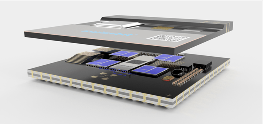
2.5 D chiplet architecture concept on PCB interposer
(courtesy of Swissbit)
A European Open Ecosystem
Simultaneously, it becomes important to create an open ecosystem for chiplet integration adapted to the European markets, moving away from the closed systems of dominant players like Intel and TSMC focussed on Computing and Datacenters. The Universal Chiplet Interconnect Express (UCIe) consortium, which includes major industry players, has laid the groundwork for standardizing die-to-die interconnects. However, for Europe, it’s crucial to break the vertical integration barrier and promote a collaborative ecosystem.
Strategic Context: Europe's Semiconductor Packaging Landscape and the Chips Act
The European industrial ecosystem in packaging consists of equipment suppliers addressing global demand and Integrated Device Manufacturers (IDMs) with capabilities that are not publicly accessible. The majority of large-volume packaging services (Outsourced Semiconductor Assembly and Test, or OSATs) are located in Asia, more specifically in Taiwan, Malaysia and China. The remaining packaging services in Europe primarily serve sovereign markets, which account for more than 50% of their activity. These providers focus on low-volume, high-value markets. European companies developing products specifically for the European market often struggle to find suppliers. European suppliers lack capacity or don’t have the technology, and Asian cannot deal with these orders due to insufficient volume commitments.
On the other end, the European Chips Act has catalyzed investments in the semiconductor sector, focusing on research, production capacity, and supply chain resilience. With a budget of €370 million dedicated to advanced packaging pilot lines.
The current situation is characterized by a strong European research community, but with limited packaging service offerings. There is a clear gap between the needs of European SMEs and the available services within Europe. One of the strategic recommendations from Pack4EU is to support the creation of Open Piloting Facilities. While research pilot lines will focus on developing technology building blocks and integrating them into demonstrators, the piloting facilities will serve as hubs for technology transfer and will adopt a product development approach in their production processes.
The required investment depends largely on the technologies to be deployed. 2.5D technology based on PCB interposers would require pushing the limits of positioning and substrate design, while silicon or glass interposers would allow for finer pitches but also necessitate equipment and processes similar to front-end manufacturing, which demand significantly higher investments.
In the European landscape of packaging services, no single entity can typically afford the investment required for such industrial tools on its own due to insufficient customer commitment. We have observed that IDMs (Integrated Device Manufacturers) can operate their own facilities when these offer a competitive advantage. Therefore, a successful deployment of a Piloting Facility would likely require a mixed business model, where a company with an IDM model opens its facilities for services and prototyping.
Pack4EU's Strategic Recommendations for Europe's Advanced Packaging Roadmap
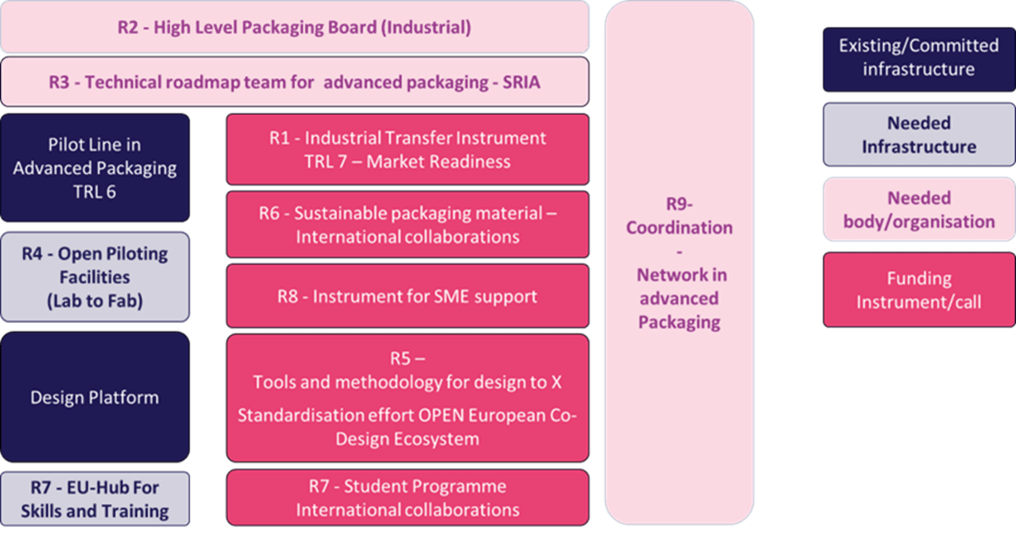
Pack4EU has identified critical areas and provided strategic recommendations to address the current gaps in Europe’s semiconductor packaging ecosystem. The recommendations are covering 3 areas:
- Needed Infrastructures
- Needed Financing Instruments
- Organisation and Governance

Pack4EU Set of recommendations
Among the needed infrastructures, the Open Piloting Facilities should be designed to support small and medium-volume production, providing an environment where companies can test, validate, and scale their advanced packaging technologies. It is also important to map and connect all the training capacity available in Europe to make them available for reskilling and upskilling.
Some adapted funding instruments are also recommended to Bridge Research and Industry with a specific industrial transfer instrument to rapidly translate research into industry-ready solutions.
Developing a European Chiplet Ecosystem: To break the current closed ecosystem dominated by a few global players, Europe needs to build an open design ecosystem for chiplets. This involves creating standardized design methodologies, simulation tools, and a marketplace for chiplets that ensure compatibility and interoperability.
Promoting Ecodesign and Sustainability: Integrating ecodesign into semiconductor packaging requires developing tools for CO2 footprint calculation and encouraging the use of sustainable materials. Europe’s focus on environmental responsibility in semiconductor manufacturing aligns with global efforts to reduce the industry’s ecological impact.
The INPHO Venture Summit is a gateway
to transforming your startup into a success story.
The INPHO Venture Summit is a gateway to transforming your startup into a success story. By connecting with investors, industry leaders, and potential partners, INPHO provides the perfect platform to showcase your innovative solutions and secure the funding necessary for growth. The summit’s comprehensive program includes pitch sessions, networking events, and one-on-one meetings, designed to facilitate meaningful connections and foster collaboration. It provides a unique platform to present your innovative solutions to a global audience, gaining the recognition needed to attract significant investment. Furthermore, the chance to secure the necessary capital to develop and scale your technology is demonstrated by the success stories of past participants.
Start-ups with innovative solutions in advanced packaging, chiplet architecture, and ecodesign are encouraged to reach out to the INPHO Venture Summit team at inpho-ventures@blumorpho.com for collaboration opportunities.
For those interested in Europe’s evolving semiconductor landscape, collaborating on advanced packaging technologies, or discussing investment opportunities, Blumorpho offers a wealth of expertise. Régis Hamelin, CTO of Blumorpho, is leading efforts to enhance Europe’s competitiveness in semiconductors through technological differentiation, sustainability, and productivity.
Contact
Regis Hamelin
hamelin@blumorpho.com
https://blumorpho.com

